


Have you ever wondered what is Netlist in PCB design? Not to worry, as you are not alone. For most people, PCB design is just confusing, and it becomes more complicated with all these technical terms like Netlist and others coming into play.
But worry not, as this article will help you. We will explain Netlists in an easy-to-understand, straightforward manner, after which you will be ready to start your PCB design projects like a pro.
So, let’s get started.
What is a Netlist?
A Netlist is just a data file that has the electrical connections existing among the various schematic diagram components. It is a file that acts like a blueprint of component arrangements, and it gives the PCB layout software the direction on how the physical arrangement of elements and connections on the board is to be completed.
For example, take building a house. Long before the actual construction can start, a thorough plan is needed in which the position of each room is shown and how they will connect through pipes and wires.
Similarly, in PCB design, the netlist serves as that blueprint, mapping out the electrical pathways between components.
Think of it as a road map for your PCB layout software. It tells the software what parts are to be connected and how to be connected so the circuit functions. It cannot do perfect component placement or trace routing effectively without a netlist.
Now you must be wondering, how the Netlist file is created. Let’s discuss this in detail.
Generating Netlists with EDA Software
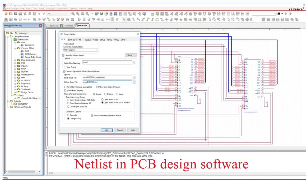
Netlists are developed by using Electronic Design Automation software like Altium Designer or Cadence Allegro. As you create your circuit schematic in these programs, the software quietly keeps track of all the connections you make.
When your schematic is ready, you simply click a button and boom. The software analyzes your schematic and puts together a list of all the connections between components. This list is your Netlist.
In short, EDA software makes the creation of netlists easy. It does all the technical stuff in the background, leaving you to concentrate on circuit design.
Utilizing Netlists in PCB Design
Netlists are very important in the entire process of PCB design. They serve as a guideline in layout to the designers as to where the components are to be located and proper trace routing.
But this is not the end of their use. Netlists also play a vital role in Design Rule Checking (DRC), ensuring that the design meets specific rules and standards.
They are helpful in simulations because a designer can use the netlist data to improve the simulation activity, which can further help in the test and validation of functionality and performance of the circuit before proceeding to make the PCB physically.
This helps in the early realization of the issues, time, and resource-saving in the future.
In short, netlists are Swiss Army Knives for PCB designers, have many functions, and enhance design efficiency and accuracy.
Netlist Formats and Compatibility
Netlists come in different formats, depending on the Electronic Design Automation software you are using. Some common formats include SPICE, EDIF, and IPC-D-356.
SPICE is quite specific to circuit simulation software that is typically used for simulation analysis. At the same time, EDIF is more general in its application and can facilitate the transfer of design data between EDA tools. On the other hand, IPC-D-356 is a standardized form of netlists used in bare-board electrical test programs.
Compatibility between these formats is essential for smooth communication and collaboration among designers using different software tools.
Ensuring that your EDA software supports importing and exporting netlists in these standard formats can streamline the design process and prevent compatibility issues down the line.
Therefore, whether you are simulating a circuit, moving designs between tools, or preparing them for electrical testing, compatible Netlist formats will ease your life.
Conclusion
So that’s all you need to know about Netlist in PCB design. With that information, you are all set to handle PCB design just like a professional.
So next time you are working on a project, Netlists won’t be a mystery anymore.