Free DFM Check for Your PCB Design
Our Free DFM Check helps you identify potential manufacturability issues in your PCB design before production. Avoid costly errors, improve design efficiency, and speed up your project timeline with our expert analysis.
Submit Your Design for a Free DFM Check
Just upload your files and we’ll have a free DFM report delivered to your inbox within 24 hours.

Why a Free DFM Check is Essential for Your PCB Design?
A Design for Manufacturability (DFM) check is a crucial step in the PCB design process, particularly for complex designs. This service helps engineers identify and rectify potential issues during the design phase that could negatively impact manufacturing. By implementing a DFM check, you can ensure a smoother production process and avoid costly mistakes later on.
Identifying Design Errors
One of the primary benefits of a DFM check is its ability to identify design errors early in the development cycle. Without this proactive approach, engineers might overlook critical issues that lead to unnecessary rework during production. Common design mistakes include incompatible component layouts and improperly sized traces, which can significantly impact the overall functionality of the PCB. By catching these errors in advance, you save time and resources, allowing for a more efficient workflow.

Improving PCB Manufacturability
A DFM check enhances the manufacturability of your PCB, ultimately reducing production delays. By optimizing your design for manufacturing, you ensure that the PCB can be produced using standard processes and techniques. This means fewer complications during assembly and a faster turnaround time from design to production. When designs are straightforward and manufacturable, manufacturers can maintain consistent quality and keep lead times short.

Lowering Manufacturing Costs
Another significant advantage of a DFM check is the potential for cost reduction. By identifying issues that could complicate the manufacturing process, you can make adjustments that optimize material usage and component layout. This not only reduces waste but also minimizes labor costs associated with fixing design flaws during production. A well-optimized PCB design translates directly into lower manufacturing expenses and improved profit margins.

Common Issues Without a DFM Check
Without a DFM check, several common problems can arise, hindering the efficiency of your PCB design:
- Incompatible Component Layouts: Designs may include components that are not compatible with each other, leading to assembly failures and increased rework.
- Trace Width Issues: Traces that are too wide or too narrow can lead to power loss, signal integrity problems, or even physical damage during manufacturing.
- Poor Pad Design: Inadequately designed pads can result in weak solder joints or improper component placement, risking overall functionality and reliability.

How Does the Free DFM Check Process Work?
Submit your Gerber files
or PCB design files.
Professional engineering team will conduct
comprehensive DFM analysis on the design
Users receive a detailed DFM report that identifies issues and provides suggestions for design optimization.
What You’ll Receive in Your Free DFM Report
- Component Layout:We will assess the spacing and arrangement of components to prevent conflicts and ensure efficient soldering.
- Routing Design:We will check if the trace width is appropriate for the expected current load and verify that there is sufficient spacing to avoid short circuits.
- Pad Design:We will evaluate the size and shape of pads to ensure reliable solder joints and prevent weak connections.
- Hole and Via Design:We will assess the size and placement of vias and holes to maintain signal integrity and manufacturability.
- Signal Integrity:We will analyze high-frequency signal paths to minimize issues such as reflection and crosstalk.
- Thermal Management:We will verify that adequate heat dissipation measures (such as heat sinks) are in place to prevent overheating.
- Material Selection:We will ensure that the selected materials are suitable for the intended application while considering dielectric properties and thermal characteristics.
- Manufacturing Process Compatibility:We will confirm that the design meets SMT or THT requirements to prevent production issues.
- Cost Assessment:We will provide an initial evaluation of material and manufacturing costs to maintain budget control.
- Additional Checks:We will review the completeness and accuracy of design documents (such as Gerber files) to minimize errors during the production process.
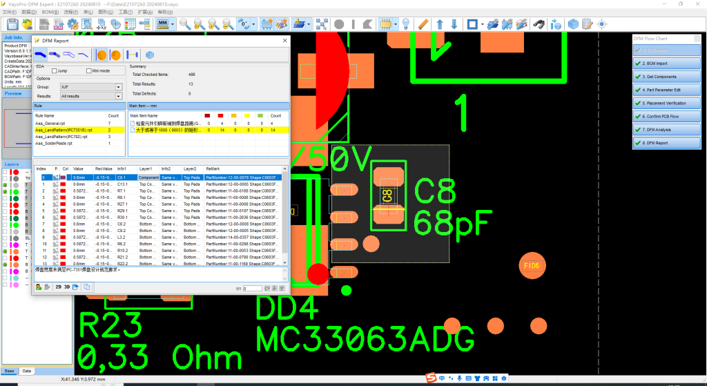
After inspection, our experts will provide design modification recommendations for these issues.The following is a sample report of our company’s free DFM inspection, which you can download and view.
See How Our Free DFM Check Has Helped Others
FAQs
You need to submit Gerber files, BOM (Bill of Materials), and any related design documents. Gerber files are used to describe the electrical layers and physical structure of the PCB, while the BOM contains detailed information of all components. This information will help us conduct a comprehensive DFM check.
1. File version and last updated time
2. Clear component number and silk screen
3. BOM including manufacturer brand and material number, description, number
4. Confirm PCB manufacturing process: material, board thickness, copper thickness, number of layers, surface treatment, character color and special process
5. Reasonable PCB layer and panel method
6. Provide correct SMT steel mesh file
7. Complete program burning and functional test plan
8. Clear finished product schematic and assembly manual
9. Other special process requirements
10. Adaptation test of BOM material and PCB pad (customer engineers often fail to update BOM in time during design changes, resulting in the purchase of wrong materials)
11. Evaluate the process of PCB circuit board, including but not limited to: processing sequence, steel mesh opening adjustment, furnace direction and carrier production, analysis of heat-absorbing large pads and peripheral components, moisture-sensitive/thermal-sensitive component protection, PCBA test plan and detection rate, trial production quantity and trial production report, etc.
Typically, you will receive feedback from DFM checks within 24 to 48 hours after submitting your design. Our engineering team will analyze your design as quickly as possible and provide detailed inspection results and improvement suggestions.
Yes, we provide DFM checking service completely free of charge, with no hidden charges. Our goal is to help you optimize your design and ensure smooth production.
Of course! If you have any questions about the inspection results or need further modifications, you are welcome to resubmit your design. We will continue to provide support based on your feedback until you are satisfied.
Our DFM inspection service is suitable for all types of PCB designs, including single-layer boards, multi-layer boards, high-frequency PCBs, and flexible circuit boards. No matter how complex your design is, we can provide professional inspections and suggestions.
We attach great importance to customer privacy and design data security. All submitted files and information will be strictly protected in our system, and only authorized engineers can access this data. In addition, we promise not to disclose your design information to any third party.

