


Worried about timely PCB designs? Well, you are not alone. Meeting deadlines can be really hard, especially for PCB design, in this fast-paced world.
But no worries at all, this article is crafted to help guide you through the PCB design process; whether you are just starting out or a seasoned pro, we have got your back.
We will walk with you to face the challenges of lead time, which affect everyone, and help you make your workflow smoother.
So, let’s get started.
PCB Designing Process Overview
To know the PCB design lead time and how to take the most from it, first, understand the overall designing process.
For this, let’s first discuss the various stages of the PCB design cycle.
Various Stages of the PCB Design Cycle
- Conceptualization: In conceptualization, shaping of ideas and looking at the feasibility, scope, requirements, and objectives of the project are defined.
- Schematic Design: Here, the circuit schematic is created, outlining the connections between components and their functions.
- Choosing Components:The success of this phase is dependent on the rational selection that allows the choice of components according to functionality, availability, and cost.
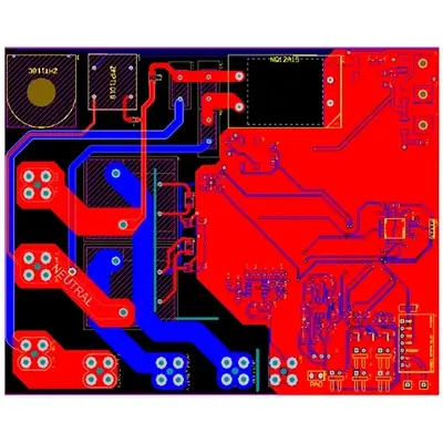
- PCB layout: Translation of the schematic information to a physical layout including all the placements of the components, trace definitions, and optimization of the printed circuit board for effectiveness and manufacturability.
- Design Verification: It is a verification test that verifies the specifications and checks only the correctness of functionality just before going to the production phase.
Now let’s discuss the main tasks and content of each stage in detail.
Main Tasks and Content of Each Stage
- Conceptualization: Defining project goals, establishing requirements, and conducting feasibility studies.
- Schematic Design:Creating circuit diagrams, symbol libraries, and establishing component connections.
- Component Selection:Researching and selecting components based on performance, availability, and cost.
- PCB Layout: The component placement, trace routing, exercises for the layer definition, and electrical performance optimization with manufacturability.
- Design Verification: This is the one that ensures the functionality of the product and conformity to the specifications through prototype, simulation, or analysis.
Understanding these stages lays the foundation for effective management of PCB design lead time.
Now let’s discuss some common factors affecting the PCB design cycle.
5 Common Factors Affecting the PCB Design Cycle
A number of factors influence the duration and effectiveness of the PCB design cycle. All the above factors are of great importance in order to properly handle the lead time.
Let’s explore the five most common ones:
1.PCB layer count
The number of layers on a PCB determines how complex and how much information it can handle. More layers usually means more design work and time.
2.Signal integrity
In high-speed digital circuits, signal integrity is a critical factor. This includes controlling signal latency, crosstalk, signal integrity, clock skew, and more. To guarantee accurate signal transmission and stability, intricate signal examination and wiring schematics are necessary, potentially leading to an extended design process.
3.Component layout
The layout of components directly affects the performance and reliability of the PCB. Enhancing the layout can minimize signal disruption, boost heat dispersion, streamline the soldering procedure, and so on. Designers need to consider things like how far apart components are, where signal wires go, how heat spreads, and more. This takes a certain amount of time to complete.
4.Solder
The soldering process has a great impact on the reliability and manufacturing cost of PCB. Designers must think about the size and shape of the pads. They also need to consider the layout of the soldering pins. This is important to guarantee high-quality and stable soldering.
5.Controlled Impedance
For high-speed digital or high-frequency circuits, maintaining controlled impedance is crucial for preserving signal integrity. To meet design requirements, we may need to use certain materials or processes to achieve controlled impedance.This increases design complexity and manufacturing costs, thus potentially extending the design cycle.
Methods to Shorten PCB Design Cycle
Going in line with the above, evidently, the designers will have the shortest lead time in the design process, based on the effective strategies applied by modern tools.
Here are several methods to expedite the PCB design cycle:
-Adopt Rapid Prototyping:
Rapid prototyping techniques, such as 3D printing and quick-turn PCB fabrication services, enable designers to iterate designs rapidly and validate concepts early in the development cycle.
This iterative approach reduces the time required for design revisions and enhances overall design quality.
-Implement Design for Manufacturing (DFM) Guidelines:
Designing with manufacturing considerations in mind can streamline the production process and minimize the risk of manufacturability issues.
Adhering to DFM guidelines, such as proper trace spacing, component placement rules, and design rule checks (DRC), ensures smooth manufacturing and reduces the need for redesigns.
-Harness Simulation and Analysis Tools:
Simulation and analysis tools allow designers to evaluate design performance, identify potential issues, and optimize designs before fabrication.
By simulating signal integrity, thermal management, and electromagnetic interference (EMI), designers can preemptively address design challenges and minimize iterations during the verification stage.
How to Estimate the Cycle Time of PCB Design Project
If you are a freelance PCB designer and your client wants to know when you are going to deliver the design, it’s essential to estimate the cycle time accurately.
Here’s a step-by-step guide to help you estimate the cycle time of a PCB design project:
1. Gather Requirements: Begin by gathering detailed requirements from the client, including project scope, specifications, desired features, and any specific constraints or deadlines.
2. Break Down the Project: Break down the project into smaller tasks or milestones, such as schematic design, PCB layout, component procurement, testing, and finalization.
3. Estimate Task Duration: Estimate the duration of each task based on factors such as complexity, resources required, and previous experience. Consider any potential dependencies or bottlenecks that may affect task completion.
4. Consider Contingencies: Factor in buffer time for unexpected delays, revisions, or unforeseen challenges that may arise during the design process. It’s essential to account for contingencies to ensure realistic estimates.
5. Allocate Resources: Determine the resources needed for each task, including personnel, software tools, equipment, and materials. Ensure that resources are allocated appropriately to meet project deadlines.
6. Sequence Tasks: Sequence the tasks in the order they need to be completed, considering any dependencies or prerequisites. This ensures a logical progression of work and minimizes idle time between tasks.
7. Review and Adjust: Review your estimates with the client to ensure alignment with their expectations and any contractual agreements. Be transparent about potential risks and discuss strategies for mitigating them.
8. Track Progress: Throughout the project, track progress against the estimated timeline and adjust as necessary based on actual performance. Regular communication with the client keeps them informed and helps manage expectations.
By following these steps, you can provide your client with a reliable estimate of the cycle time for their PCB design project. Effective estimation not only instills confidence in your abilities as a designer but also fosters trust and transparency in your client relationships.
Choose a Suitable PCB Design Service Provider
If you are a project manager or an individual seeking PCB design services, selecting the right service provider is crucial for the success of your project.
Here are some of the top PCB design companies that you may choose:
Keep Best PCBA:We have a strong design team that can design the PCB products you want for you。
Altium: Known for its advanced PCB design software, Altiumalso offers PCB design services provided by experienced engineers. They cater to various industries and offer comprehensive design solutions.
Cadence Design Systems: Cadenceoffers a range of PCB design services tailored to different project needs. Their Allegro PCB design platform is widely used in the industry, and their service team is skilled in handling intricate design requirements.
Advanced Circuits: Known for their quick turn-around time and cost-effective solutions, Advanced Circuitsprovides PCB design services along with PCB fabrication and assembly. They focus on delivering high-quality designs within tight deadlines.
Saturn PCB Design: Saturnspecializes in providing PCB design services for high-speed and RF applications. They have a team of experienced engineers capable of handling complex design challenges, ensuring optimal performance and reliability.
Zuken: Zukenprovides PCB design services leveraging their CR-8000 platform, which integrates electrical, thermal, and mechanical design aspects. They offer comprehensive design solutions tailored to the needs of different industries.